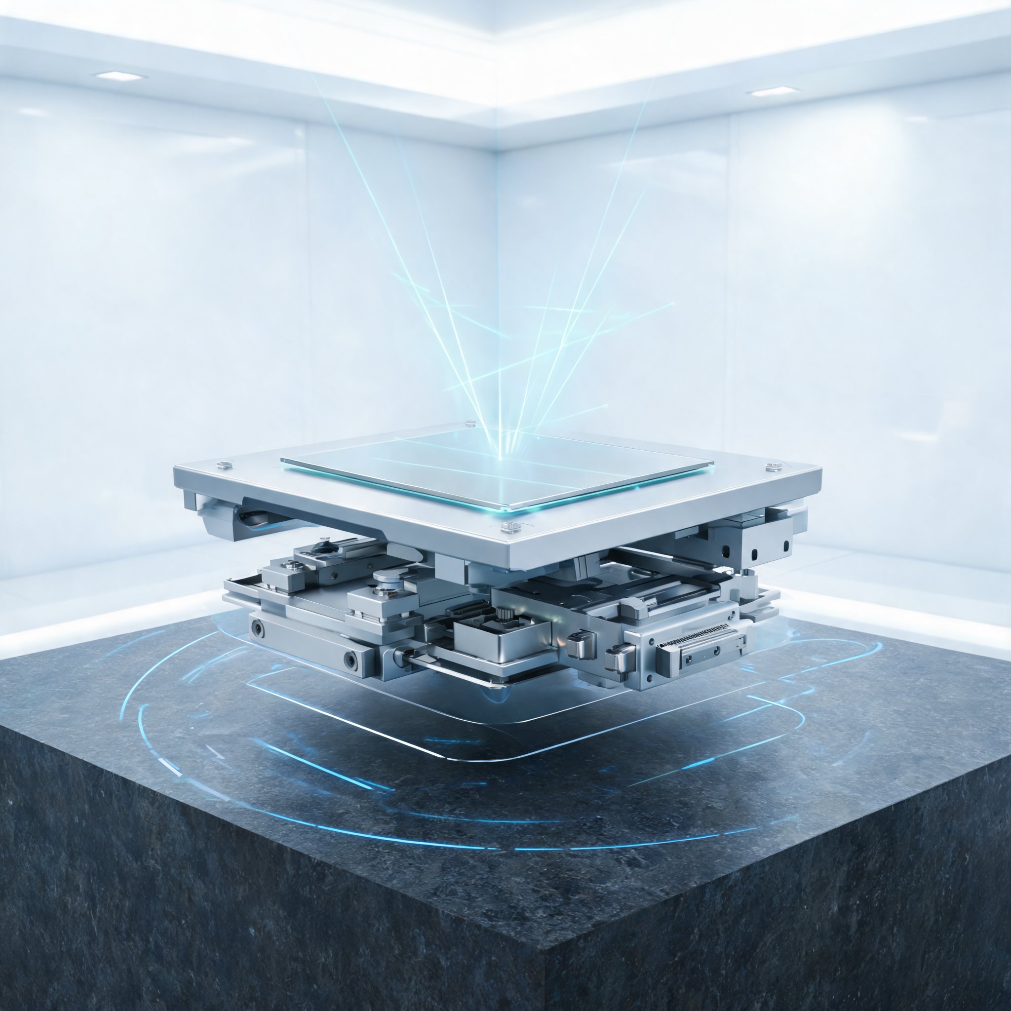
ETEL, part of HEIDENHAIN and a supplier of high-performance motion-control components and complete motion platforms, has introduced the METIS HP, a full air-bearing planar platform for demanding step-and-scan semiconductor applications. The company is targeting direct laser writing and high-resolution optical inspection systems, where precise motion and stable scanning are central to tool performance.
According to ETEL, the METIS HP is intended to combine high speed and stability with outstanding dynamic straightness and projected tool-point measurement capability. The platform is positioned as an addition to the company’s high-precision motion-control portfolio.
Encoder and trigger architecture
At the core of the METIS HP is a multi-degree-of-freedom (mDoF) HEIDENHAIN encoder. ETEL says this architecture ensures accuracy without thermal drift and enables projected tool-point measurement. The company’s controllers can emulate a transistor-transistor logic (TTL) position signal for use as a trigger event.
ETEL describes this approach as an alternative to the classical interferometer used as an advanced trigger generator. With the METIS HP, the company says there is no need to add a mirror on the carriage, no air-lensing effect or air perturbation, and a lower cost. ETEL presents these as design advantages of the platform.
Accuracy, speed and dynamic performance
ETEL lists ±150 nm accuracy over the full XY stroke after mapping and ±150 nm dynamic straightness at speeds up to 1 m/s. The platform also has dynamic capabilities reaching accelerations up to 20 m/s². According to the company, these capabilities minimize turnaround time and thereby increase machine throughput for step-and-scan applications.
For high-end inspection applications in advanced packaging, rapid and precise focal-distance adjustments are required. The METIS HP includes a high-bandwidth 4-DoF module that provides fine control over the Z, tip, tilt and theta axes. ETEL positions the platform as suitable for these demanding inspection tasks.
Large substrates and maskless lithography
The platform supports panel sizes up to 600 mm × 600 mm. ETEL says this addresses the growing need for next-generation maskless lithography with large-area substrates.
“Building on ETEL’s long-standing expertise in high-precision platforms, the METIS HP provides the trajectory quality required for advanced optical processes,” said Stéphane Pellegrini, Product Manager at ETEL. He added that its speed stability and dynamic straightness are intended to ensure consistent performance even at high scanning velocities.
The METIS HP is therefore presented as a motion platform for semiconductor scanning, laser writing and inspection workflows that require tight positioning, stable dynamics and large substrate handling. The announcement focuses on the platform’s specifications and target applications.